Gurmeet Singh
Sunnyvale, CA 94086
https://www.linkedin.com/in/gurmeet
https://github.com
Summary
I have extensive and broad experience in Physical Design and a long history of successful, productized tapeouts, sometimes using flows that I set up. (U.S.Citizen.)
Professional Experience
[2022-2024] Intel Corp., Physical Design Methodology Engineer
- Set up and use an implementation (rtl2gds) flow for Intel 18A node using Cadence Flowtool that supports numerous flow, technology, power/performance/area optimization options. This enabled batch jobs with up to thousands of parallel runs with different options, IPs, libraries and metal stacks for regressions or analysis. Started the git repo for the flow and made over 150 commits.
- Worked with Cadence to productize an Intel18A PPA oriented reference flow usable by customers to jump start their own implementation flows.
- Set up infrastructure for analyzing a large number of Intel18A synthesis/place&route runs on industry standard IPs with Cadence based Genus/Innovus based flow, collect PPA and other QOR metrics and continually document/present them visually using Python-Matplotlib and R-ggplot2.
- Use the above infrastructure to continually improve and benchmark the PPA metrics of industry standard IPs and publish results with different versions of Intel18A libraries and PDKs.
- Worked with Cadence to produce a performance optimized implementation and the associated hierarchical RTL2GDS flow for a high performance ARM core (Cortex-X925 “Blackhawk”) on the Intel18A process.
[2020-2022] Samsung Austin R&D Center, Physical Design Contractor
- Physical implementation (rtl2gds) of 3 large GPU blocks to tapeout [Silicon Success] on a 4nm technology using Cadence Innovus, including floorplanning in SNPS, meeting all area/power/timing requirements. Over 75 timing/DRC ECOs. Provide guidance to the CAD team on methodology.
- PnR flow development in SNPS fusion compiler for 3nm (Samsung 3GAP) technology
[2018-2019] Esperanto Technologies, Physical Design Methodology and Global Clocking Engineer
- Defined physical design methodology for 7nm process corners including very low voltage operation and timing margins
- Design of global clock distribution network for a very large 7nm SoC, model the reconvergent network, simulate with spice, implement using ICC2 and resimulate with extracted spice netlist. Publish chip level clock specification document.
- Block level place and route implementation of a million gate low voltage design.
- Set up a Synopsys Custom Compiler schematic and netlisting environment with extracted views. Characterize PVT sensitivity of library cells, esp. level shifters and a ring oscillator with spice simulations and publish results.
- Set up and define methodology for an EM/IR flow using Ansys Redhawk/Seascape
- Support and manage PLL, DLL, DDR, PCIE vendors through weekly meetings.
[2015-2017] ZGlue Inc., Physical Design (Independent Consultant)
- Physical design methodology and netlist-to-gds flow development in tcl using Cadence toolset. Also developed Assura physical verification and logical equivalence (lec) flows.
- Hierarchical implementation of an instance array design including floorplanning, power grid design, pin placement, place and route, logical equivalence and physical verification. Silicon success.
- Abstract (LEF) generation of analog macros and hierarchical instances to allow for through the block routing.
- Mixed-signal custom CAD support including SKILL programming
- Set up Virtuoso QRC extraction flow for full chip STA, set up and run full chip STA with Tempus, set up and run full chip LEC with Conformal. Silicon success.
[2015-present] Machine Learning/AI
- Several courses on deeplearning.ai
- Data Science/Machine Learning.
- Kaggle Participant
- CNN, RNNs, XGBoost.
- Tensorflow, Keras, numpy, sklearn.
- Python, R. Bit of Scala, Swift, MATLAB.
- Expert linux user.
[2013-14] Qualcomm Technologies, Senior Staff Engineer
- 40nm ASIC: Top level floorplan and power grid design with multiple power domains for a mixed signal design, automated floorplan generation with Tcl. Wrote power intent CPF from scratch. Full chip formal (LEC) and low power (CLP) verification using Cadence tools. Apache Redhawk EM/IR debug and fixes. Received Qualstar certificates. Beat the schedule.Silicon success (WCD9335).
[12-13] Cadence Design Systems, Staff Applications Engineer
- Developed complete, automated rtl2gds flow (Globalfoundries 14nm/finFET); optimized for PPA and validated on A9 ARM core with Neon coprocessor (TT Nominal @ 2.5 GHz).
- Helped tapeout a DDR IP for a client by doing the final setup/hold/other fixes.
[2011-12] Sandforce Inc./LSI Corp., Principal Physical Design Engineer
- Developed a complete, and deployed, a 40 nm automated and optimized, tapeout ready, Cadence based netlist to tapeout implementation flow at Sandforce Inc.
- Wrote Tcl scripts for a correct by construction, tunable flow used to implement all blocks in the design.
- Developed automated, tapeout ready, STA setup using Primetime-SI using Tcl/Perl scripts.
- Did studies on standard cell EM limits by frequency and flip-flop metastability
- Implemented eight large blocks at tapeout quality using the above flow ; the resulting GDSII were timing, LEC, LVS/DRC clean. Silicon success.
- Helped grow the size and capability of the physical design team and lead technical direction.
[2010-11] West Valley Technologies (Physical Design Contractor at Sandisk)
- Set up 40nm Cadence based, automated, tapeout ready, block level netlist to tapeout implementation flow at Sandisk Inc.
- Developed hierarchical physical implementation flow in 65nm technology using Cadence at Sandisk.
[2008-10] Qualcomm, Independent Contractor for Physical Design
- 65nm WiFi ASIC: Tapeout implementation of large block using Magma. Silicon Success.
- 65nm WiFi ASIC: Full chip EM/IR signoff using Apache-Redhawk. Silicon Success. Silicon Success.
[2007-08] AMCC, Principal Engineer
- Telecom ASIC: Tapeout implementation of two large blocks using Magma at AMCC. Silicon Success.
- Set up 65nm Cadence Encounter based block level implementation flow.
[2006-07] Teranetics, Principal Engineer
- 130nm/65nm 10GBASE-T Phy ASIC: Implement many large blocks to tapeout, some using x-route.
- Automate implementation flow using Magma Blastfusion place and route tool, static timing analysis flow, logical equivalence flow and physical verification flow.
- Power estimation; power reduction using special cells. Silicon Success.
[2004-06] Airgo Networks, Physical Design Manager
- Multiple WiFi ASICs: Implement many blocks using Magma. Automate PTSI STA, formal (LEC) and Calibre physical verificatino flows.
- Full chip EM/IR flow development and signoff using Apache-Redhawk.
- Tapeout signoff/jobview. Multiple ECOs, I/O Spice sims and silicon failure analysis, IP integration, Methodology, project management. Silicon success.
[2001-04] Transmeta, Senior Member of Technical Staff
- 1.2/1.8GHz Efficeon CPUs: Implement Hyper-Transport PnR blocks; Silicon Success. efficeon1
- Register File custom circuit design. Silicon Success. efficeon2
- Peformed dozens of all layer and metal-only ECOs.
- Setup latch compatible STA flow. Array and noise methodologies.
- One patent awarded on a Repeater Circuit.
[1999-01] Sun Microsystems, Member of Technical Staff
- UltraSparc V CPU: CAM Register File (4 write, 2 read, 1 compare) design, modeling and verification
- 1.2GHz UltraSparc III CPU: Ported a dozen 130nm dynamic circuit blocks, including adders up to 64-bits, from 180nm to 130nm. Wrote a C language module to create a timing model through Pathmill API. Silicon success.
[1997-99] Intel Corporation, Design Engineer
- 833MHz Pentium III Xeon CPU: High speed dynamic circuit design for L2$ ECC, L2$ STA/EM/IR verification. Silicon success.
- 600 MHz Pentium III CPU : GTL I/O circuit design. One patent disclosure. Silicon success.
[1994-97] STMicroelectronics, Design Engineer
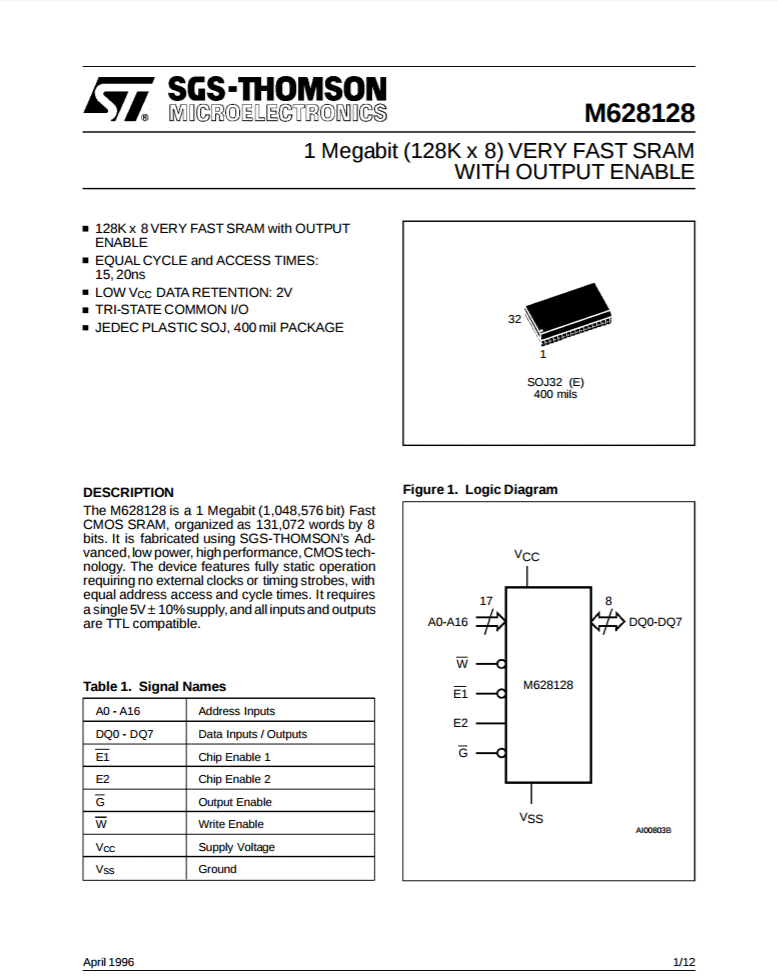
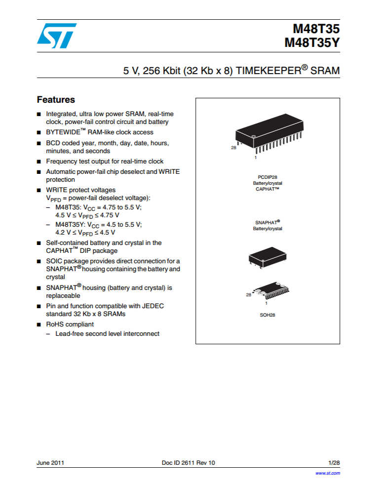
- Circuit Design of a high performance 32kx8, and a low power 128kx8 SRAM. Silicon success. CAD setup for custom circuit design. Reverse engineer a competitor register file and re-implement, verify functionality (including leap years, Y2K etc.) using verilog switch level simulation. Silicon success.
Education:
[2015-2018]: Coursera Courses
- Neural Networks and Deep Learning [Code]
- Machine Learning [Code]
- Machine Learning With Big Data
- Practical Machine Learning
- Structuring Machine Learning Projects
- Improving Deep Neural Networks: Hyperparameter tuning, Regularization and Optimization
- Convolutional Neural Networks
- Sequence Models
- How Google does Machine Learning
- Launching into Machine Learning
- Intro to TensorFlow
- R Programming
- Statistical Inference
- Reproducible Research
- Regression Models
- Functional Programming Principles in Scala
- Object Oriented Programming in Java
- Financial Markets
- Graph Analytics for Big Data
- Hadoop Platform and Application Framework
- The Data Scientist’s Toolbox
- Getting and Cleaning Data
- Exploratory Data Analysis
- Developing Data Products
- Introduction to Big Data
- Introduction to Big Data Analytics
- HTML, CSS and Javascript for Web Developers